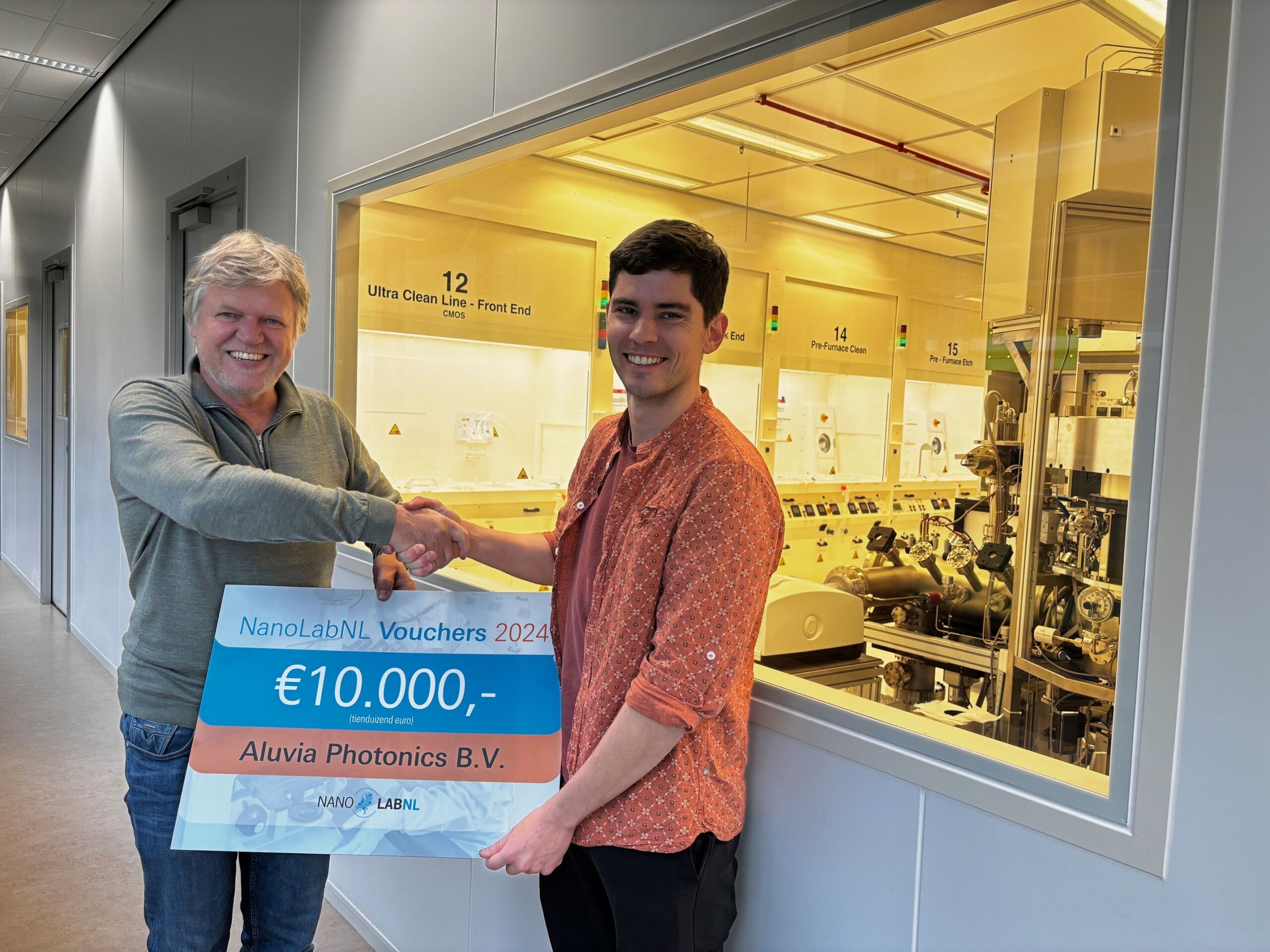
In November 2024, Guus Rijnders presented Michiel de Goede, Principal Engineer of ALUVIA Photonics, with a NanoLabNL voucher. This voucher enables ALUVIA Photonics to redeem hours in the cleanroom of the MESA+ NanoLab, located in Enschede, for comprehensive training, expert guidance, and the use of cutting-edge equipment.
Michiel: “Thanks to the support from NanoLabNL, Aluvia Photonics is able to advance its fabrication process to commercialize Al2O3 photonic integrated circuits. More specifically, the voucher will be used to further develop key fabrication processes of our multi-project wafer (MPW) services”.
Al2O3 MPW processing
The project for which ALUVIA requested a voucher aims to fabricate photonic chips based on the Al2O3 photonic material platform. The users will introduce themselves to the relevant equipment and the processing steps for producing photonic chips. The fabrication process will be used in future R&D and commercial projects to deliver similar photonic chips in the future to a variety of partners as part of their MPW services.
About ALUVIA Photonics
ALUVIA Photonics provides photonic integrated circuits (PICs) on the Al2O3 integrated photonic platform. The unique selling points of the technology are:
- Broad operating spectral window ranging from 200 nm till the mid-IR (~3 um)
- Very low propagation losses
- Possibility of optical amplification by rare-earth ion doping of the material.
PICs can be accessed via both dedicated and multi-project wafer (MPW) runs.
For more information about ALUVIA Photonics, please visit their website.
