Photonic topological insulators are currently at the forefront of on-chip photonic research due to their potential for loss-free information transport. Realized in photonic crystals, they enable robust propagation of optical states along domain walls. But how robust is robust? In order to answer this, researchers from AMOLF and TU Delft used near-field optical microscopy to quantify photonic edge state transport in silicon photonic crystals made in the AMOLF NanoLab Amsterdam. The findings provide a crucial step towards error-free integrated photonic quantum networks. The results were published in the journal Light Science & Applications.
Topologically tailored photonic crystals have opened up the possibility for attaining robust unidirectional transport of photonic signals. The unprecedented guiding capabilities – supporting unhindered transport around imperfections and sharp corners without the need for any optimization – are highly beneficial for efficient distribution of information through dense on-chip photonic networks at telecom wavelengths. However, transport properties of such topologically non-trivial states have so far only been inferred by transmission measurements, and quantification of robustness remains challenging.
Creating and combining topological photonic crystals
In a new paper published in Light: Science & Applications, a team of researchers led by Kobus Kuipers (Delft University of Technology) and Ewold Verhagen (AMOLF), reports a rigorous robustness evaluation of photonic edge eigenstates at telecom wavelengths. Using the high-resolution electron beam lithography and reactive ion etching facilities of the Amsterdam NanoLab they fabricated a topological photonic crystal. This crystal consists of triangular holes perforating a silicon membrane. Due to the two different hole sizes, the mathematical description of light waves propagating in the crystal acquires a special structure, or ‘topology’.
Then, when two crystals with different arrangements of the smaller and larger holes are brought together, the boundary between both crystals supports a light wave that has intriguing properties; it can flow unhindered around any sharp corner of the boundary. At TU Delft the researchers visualized those photonic edge states in the photonic chip with a phase-resolved near-field optical microscope. The technique allowed them to separate forward propagating light from backward travelling waves with extreme sensitivity and thus perform local monitoring of back-scattering along the domain wall.
Light waves flowing unhindered around sharp corners
The researchers further complemented their quantitative analysis of the topological edge waves with light waves propagating in an ordinary photonic crystal waveguide. They found that in stark contrast to the waves in the topological crystal, the light in the ordinary crystal shows significant loss across a ‘defect’, consisting of four sharp waveguide corners. The light waves are scattered to a back-reflected wave. The topological waves instead flow around the sharp corners seemingly unhindered. The researchers were able to conclude that the topological protection reduces the back-reflection from an individual corner by two orders of magnitude for all optical frequencies.
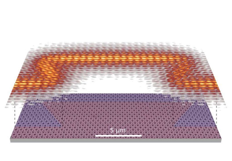
Experimental visualization of light propagation
Reference
Sonakshi Arora, Thomas Bauer, René Barczyk, Ewold Verhagen and L. Kuipers, Direct quantification of topological protection in symmetry-protected photonic edge states at telecom wavelengths, Light: Science & Applications, 10, 9 (2021).