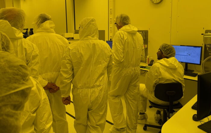
We would like to share some exciting developments that are going on at TU/e’s NanoLab. In 2023, several new equipment have become available for cleanroom users. In this news item, you will find an overview of the equipment. Besides that, ASML and TU/e announced a new phase in their longstanding partnership: there are plans for a new state-of-the-art cleanroom.
New cleanroom
The new phase in the partnership of ASML and TU/e includes a jointly defined research program, the construction of a new ASML research facility on the TU/e campus, and the creation of a state-of-the-art cleanroom. Apart from a cleanroom of 1200 m2, it should comprise an analysis lab and a packaging lab. It is envisaged to be located on the east side of the TU/e campus.
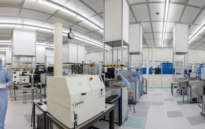
New equipment
NanoLabTUe has fully transferred it’s process line from 3” to 100 mm diameter substrates. As this wafer size is also used in the other NanoLabs, it will make the TUe process capabilities better compliant with the others and ease wafer exchange across the labs. In 2023, several new tools have become available to our users.

Spectroscopic Ellipsometer
A new spectroscopic ellipsometer (Woollam W3-03) has been installed. It features a spectral range of 245 – 1690 nm) and max. 200×200 mm scan range.

RTA
A new RTA by the company AnnealSys is operational and has replaced the old Jipelec InP tool. This machine is dedicated for annealing of III-V semiconductor materials.

Direct write laser lithography
A Heidelberg MLA-150 direct write lithography system has been installed in the cleanroom in January. The tool is equipped with a 375 nm laser, a high quality write mode that can achieve down to 0.6 um minimum feature size on isolated features, cassette-to-cassette handling, and back-side alignment. Overlay performance is expected to be 1000 nm with back-side alignment, 500 nm with frontside global alignment and down to 250 nm with local alignment. Expected write times are roughly 30 minutes for a 4-inch wafer with full wafer area designs, but up to 2.5 hours with field by field written designs.

HMD primer unit
Our old HMDS primer oven is replaced by a new primer hotplate by Sawatec.